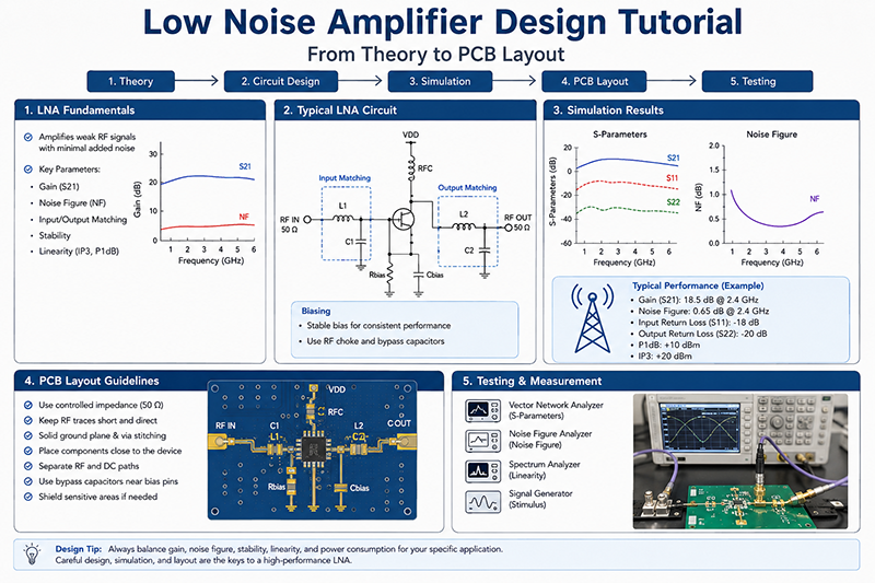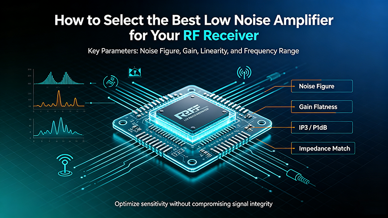


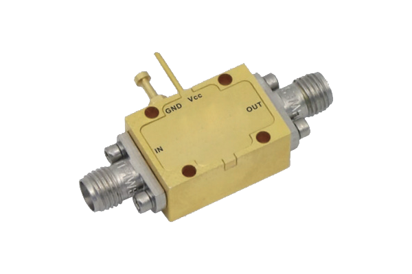
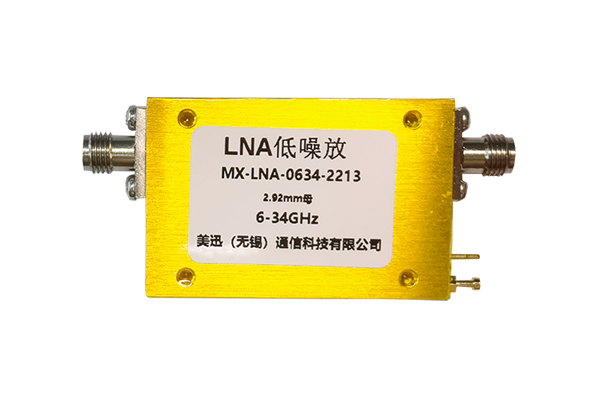




A low noise amplifier (LNA) is one of the most critical components in RF and microwave systems, especially in applications such as wireless communication, radar, satellite receivers, and test equipment. The noise figure of an LNA directly affects the sensitivity and overall performance of a receiver system.
Improving noise figure requires careful optimization of semiconductor selection, impedance matching, circuit layout, bias conditions, and system-level design. This guide explains practical methods to reduce noise figure and achieve higher-performance low noise amplifier circuits.
What Is Noise Figure in a Low Noise Amplifier?
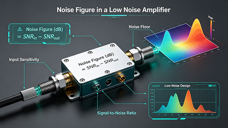
Noise figure (NF) is a measurement that describes how much noise an amplifier adds to an input signal. It compares the signal-to-noise ratio (SNR) at the input and output of an RF amplifier.
The noise figure formula is:
NF = 10 × log10 (Input SNR / Output SNR)
A lower noise figure indicates that the amplifier introduces less additional noise and preserves the quality of weak RF signals.
| Application | Typical LNA Noise Figure |
|---|---|
| Consumer Wireless Devices | 1.5 - 3 dB |
| Satellite Communication | 0.5 - 2 dB |
| Radar Systems | 1 - 3 dB |
| High Performance RF Receivers | Below 1 dB |
1. Choose a Low Noise Transistor or RF Device
The active device is the foundation of LNA performance. Selecting a transistor with optimized noise characteristics is the first step toward achieving a low noise figure.
Important Device Parameters
- Minimum Noise Figure (NFmin): The lowest achievable noise performance of the device.
- Gain: Higher gain helps improve system noise performance.
- Operating Frequency: Select devices designed for the target frequency range.
- Linearity: High linearity prevents distortion from strong signals.
Modern RF LNAs often use GaAs, GaN, or SiGe semiconductor technologies because they provide excellent noise performance at microwave frequencies.
2. Optimize Input Impedance Matching
Unlike power amplifiers, LNAs are not always designed for maximum power transfer. The input matching network should be optimized for minimum noise figure while maintaining sufficient gain.
The best noise performance usually occurs at the transistor's optimal noise impedance rather than the standard 50-ohm impedance point.
Common Matching Components
- Microstrip transmission lines
- LC matching networks
- RF inductors and capacitors
- Impedance transformation networks
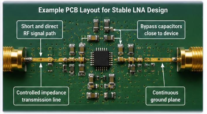
3. Improve PCB Layout Design
Poor PCB layout can significantly increase noise figure even when using a high-performance RF device. At high frequencies, parasitic effects become a major factor.
PCB Layout Optimization Tips
- Keep RF signal paths short and direct.
- Use continuous ground planes.
- Place bypass capacitors close to power pins.
- Minimize unwanted coupling between input and output.
- Use high-quality low-loss PCB materials.
4. Optimize Bias Conditions
The operating voltage and current of an LNA transistor directly affect noise performance. Incorrect biasing can increase noise figure and reduce gain.
Designers should carefully select drain current and voltage conditions based on manufacturer recommendations and measured RF performance.
5. Reduce Power Supply Noise
Power supply noise can enter the RF signal path and degrade amplifier performance. A clean and stable power supply is essential for low noise applications.
Power Filtering Methods
- Use low-noise voltage regulators.
- Add RF bypass capacitors.
- Use ferrite beads for noise isolation.
- Separate analog and digital power paths.
6. Increase Gain at the First Receiver Stage
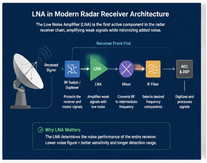
According to Friis' noise formula, the first stage of a receiver chain has the greatest impact on overall system noise performance.
A high-performance LNA placed immediately after the antenna can significantly reduce the noise contribution from later stages.
7. Minimize Loss Before the LNA
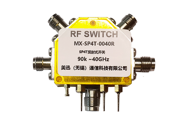
Any loss before the LNA directly increases system noise figure. Components such as cables, connectors, filters, and switches should have minimal insertion loss.
Ways to Reduce Front-End Loss
- Use low-loss RF cables.
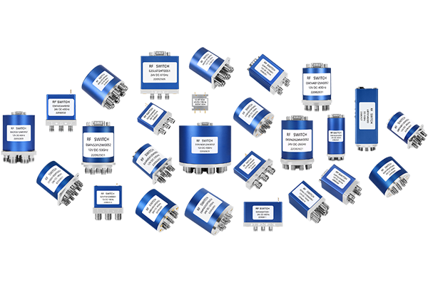
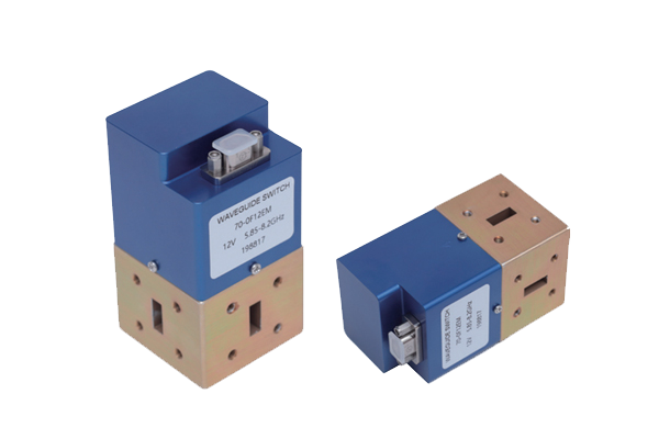
- Select high-performance RF switches.
- Optimize antenna connections.
- Place the LNA close to the antenna.
8. Use Simulation Tools for Optimization
RF simulation software helps engineers predict noise performance before hardware fabrication. Tools such as Keysight ADS, Cadence AWR, and CST Studio Suite are commonly used for LNA design.
Simulation Parameters
- Noise figure analysis
- S-parameter simulation
- Gain stability analysis
- Input/output matching optimization
Common Causes of Poor LNA Noise Figure
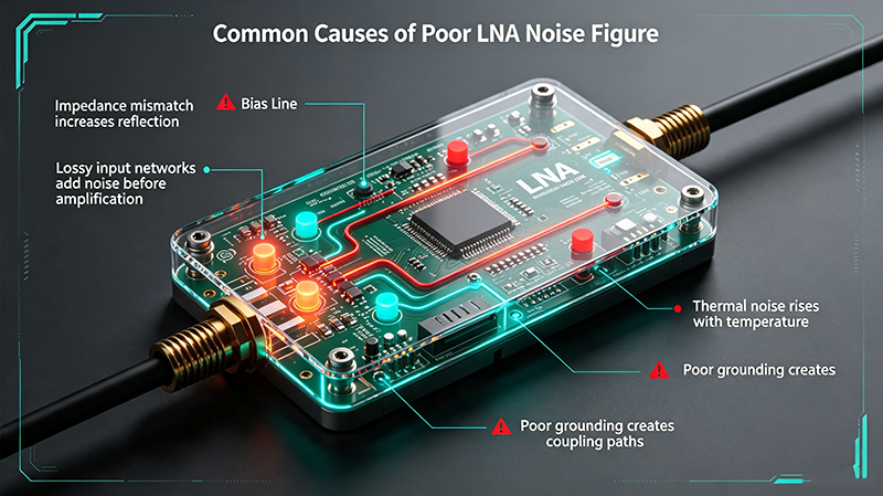
| Problem | Effect |
|---|---|
| Poor impedance matching | Higher noise figure and lower gain |
| Long RF traces | Additional insertion loss |
| Noisy power supply | Signal degradation |
| Incorrect transistor bias | Reduced RF performance |
| High-loss components | Reduced receiver sensitivity |
How to Measure LNA Noise Figure
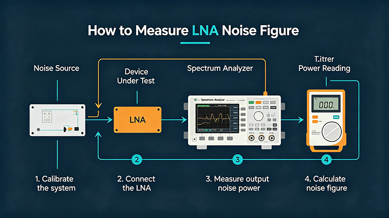
Noise figure measurements are typically performed using a noise figure analyzer and calibrated RF measurement equipment.
The measurement process usually includes:
- Calibrating the measurement system.
- Connecting the LNA under test.
- Applying a known noise source.
- Recording noise figure and gain results.
Conclusion
Improving the noise figure of a low noise amplifier requires a combination of proper device selection, optimized impedance matching, high-quality PCB design, clean power management, and accurate RF simulation.
For modern RF communication systems, achieving the lowest possible noise figure is essential for improving receiver sensitivity and maintaining reliable performance in challenging signal environments.