






What is a Bias Tee and How Does It Work in RF Circuits
Table of Contents
- 1. What Is a Bias Tee?
- 2. How Does a Bias Tee Work?
- 3. Internal Architecture
- 4. Types of Bias Tees
- 5. Key Specifications Explained
- 6. Typical Applications
- 7. How to Select the Right Bias Tee
- 8. Common Pitfalls to Avoid
- 9. Frequently Asked Questions
- 10. Bias Tee Circuit Diagram
- 11. Bias Tee Circuit Design
- 12. Bias Tee Frequency Response
- 13. Bias Tee Insertion Loss
- 14. Bias Tee vs DC Block
- 15. Bias Tee in RF Amplifiers
- 16. Bias Tee in SDR
- 17. Conclusion
1. What Is a Bias Tee?
A bias tee (often written bias-T) is a three-port passive component used to inject DC power into an RF signal path without disturbing the RF signal itself. Its three ports are:
- RF + DC port (common port) — carries both RF and DC.
- RF-only port — passes RF but blocks DC.
- DC-only port — passes DC but blocks RF.
The bias tee allows a single coaxial cable to deliver both RF signal and DC bias to a remote device — dramatically simplifying cabling in antenna towers, test racks, and microwave modules.
2. How Does a Bias Tee Work?
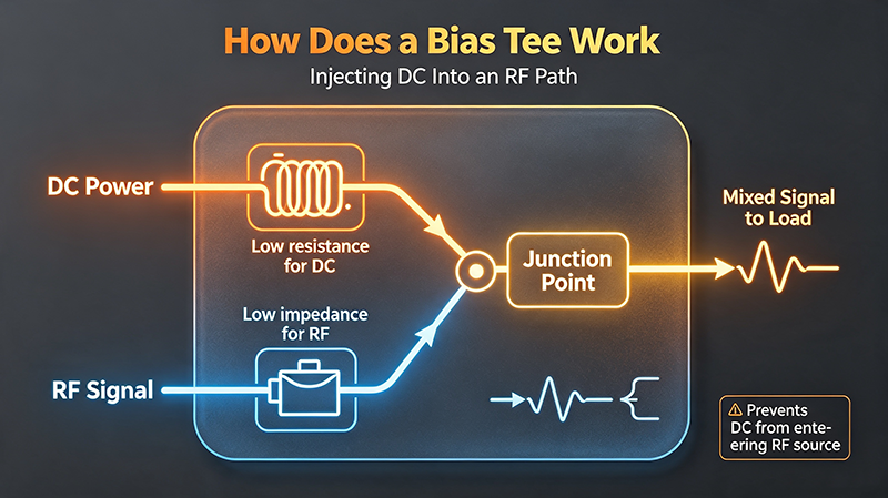
The bias tee uses two complementary passive elements:
- An inductor (L) in the DC path — passes DC freely but blocks high-frequency RF.
- A capacitor (C) in the RF path — passes RF but blocks DC.
This low-pass + high-pass filter combination lets DC and RF coexist on the same line and then separates them at the output. The RF port is isolated from DC, and the DC port is isolated from RF.
3. Internal Architecture
3.1 L-C Topology
The classic bias tee consists of a series inductor on the DC port and a series capacitor on the RF port. Together they form a diplexer that splits the signal at each port by frequency.
3.2 Lumped vs. Distributed
At low frequencies (HF/VHF), discrete inductors and capacitors are used. At microwave frequencies, the same function is implemented with microstrip or stripline sections that behave as lumped elements.
3.3 Self-Bias vs. External Bias
Some bias tees include internal regulation or filtering circuits; others are purely passive and rely on an external DC supply. Active bias tees add transistors for current limiting, monitoring, or temperature compensation.
4. Types of Bias Tees
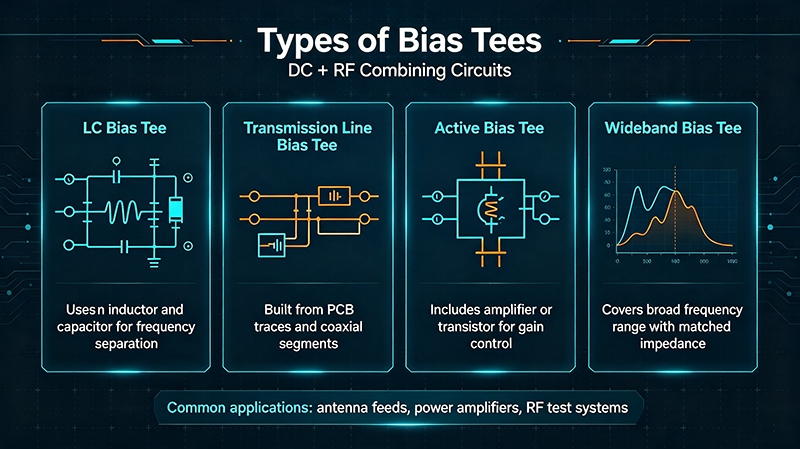
4.1 Resistive Bias Tee
Uses a resistor at the DC port to limit current. Simple and broadband, but dissipates power and adds loss.
4.2 Reactive (L-C) Bias Tee
The most common type. Uses inductors and capacitors for lossless combining. Wideband, low loss, and high isolation between ports.
4.3 Active Bias Tee
Includes active components (transistors, op-amps) for current regulation, sequencing, or noise filtering. Used where precise bias control is required.
4.4 Surface-Mount Bias Tee
Miniature chip-level bias tees for PCBs and module integration. Available in SMT packages from DC to 6 GHz or higher.
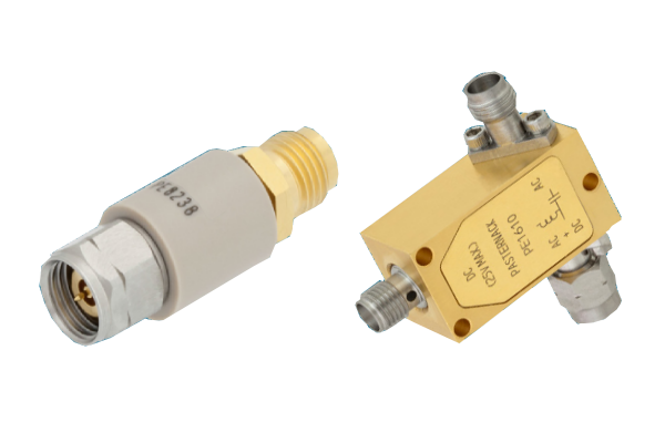
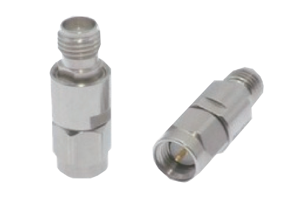
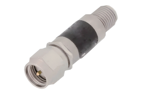
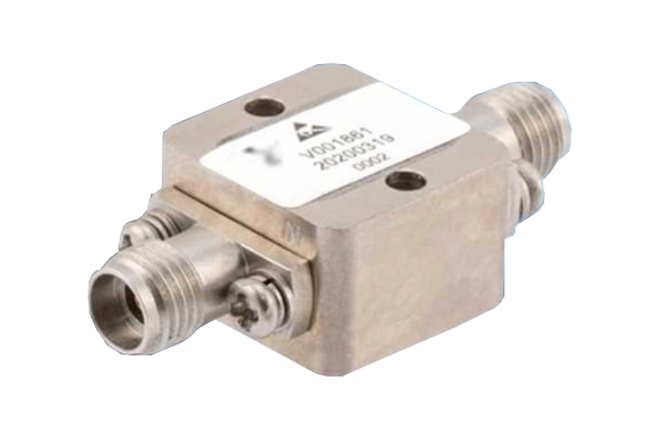
4.5 Connectorized Bias Tee
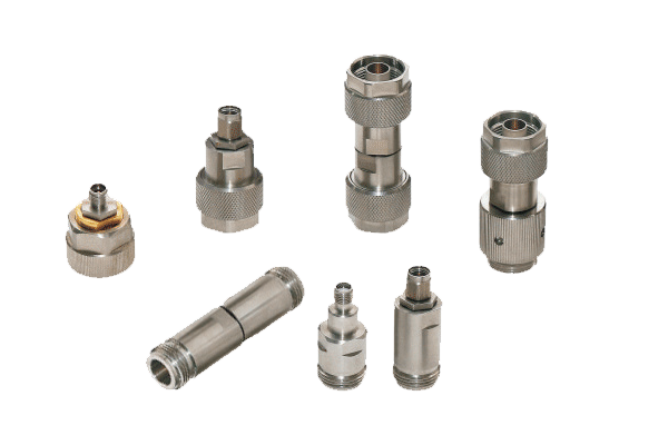
Coaxial SMA, N-Type, or BNC bias tees for bench testing and lab use. Often rated to multi-GHz frequencies.
| Type | Frequency | Insertion Loss | DC Current | Best Use |
|---|---|---|---|---|
| Reactive (L-C) | 1 MHz–50 GHz | 0.2–1.0 dB | Up to 5 A | General purpose, lab & field |
| Resistive | DC–6 GHz | 3–6 dB | < 100 mA | Low-current test |
| Active | DC–10 GHz | 1–3 dB | Programmable | Sequenced amplifier bias |
| Surface-mount | DC–6 GHz | 0.3–0.8 dB | Up to 500 mA | PCB integration |
| Connectorized | DC–40 GHz | 0.4–1.5 dB | Up to 3 A | Lab & production test |
5. Key Specifications Explained
Frequency Range
The band over which the bias tee maintains low RF insertion loss. From DC-1 GHz for simple designs to DC-40 GHz for microwave models.
Insertion Loss
RF loss between the RF port and the common port. Should be < 0.5 dB for low-loss designs.
RF-DC Isolation
How well the RF port is isolated from DC. Typically > 30 dB at center frequency.
DC Current
Maximum continuous DC current the inductor branch can handle, typically 0.5–5 A.
DC Voltage
Maximum DC voltage rating, typically 25–100 V.
VSWR / Return Loss
Impedance match at all ports. > 15 dB return loss is typical.
Rise Time / Group Delay
Important for high-speed pulsed bias, especially in radar T/R modules.
Power Handling
Maximum RF input power. Typically 1–10 W CW for passive bias tees.
6. Typical Applications
- Remote antenna powering — DC bias travels up the same coax that carries RF to an LNA on a tower.
- Active antenna biasing — powering LNAs, PAs, and filters in antenna units.
- Vector network analyzer (VNA) testing — biasing DUTs through the test port.
- Radar T/R modules — gating and biasing pulsed PAs and LNAs.
- PIN-diode switch drivers — DC control routed via bias tee.
- Photonics / optical modulators — biasing electro-optic modulators.
- Satellite ground equipment — LNA bias on long coax runs.
7. How to Select the Right Bias Tee
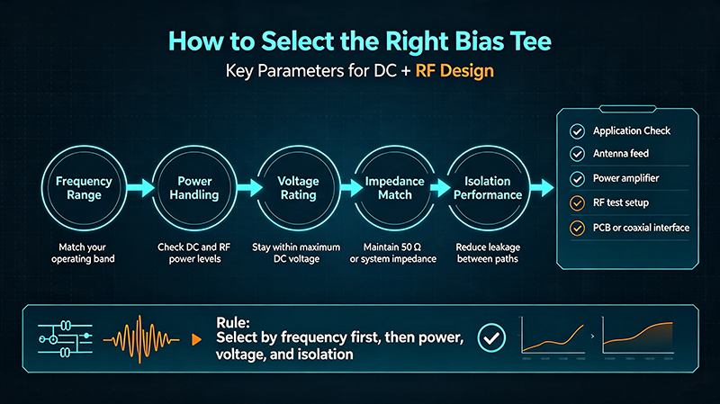
- Define the RF frequency band. Must cover your full operating range, not just center.
- Determine the DC current and voltage. Sum the worst-case consumption of all downstream devices.
- Set the insertion loss budget. Sub-1 dB is typical; less than 0.5 dB for sensitive receiver chains.
- Check the connector type. SMA, N-Type, BNC, or 2.92 mm depending on frequency.
- Choose topology. Reactive for low loss; active for regulation; surface-mount for PCB.
- Verify isolation. At least 30 dB RF-DC isolation at your operating frequency.
- Confirm power handling. Include 1.5×–2× margin for peak pulses.
- Consider environmental specs. Temperature, humidity, vibration, and altitude.
8. Common Pitfalls to Avoid
- DC short into RF port: Always check the DC port is properly blocked — a failed capacitor can short DC into the RF path.
- Insufficient current rating: The inductor saturates and impedance drops above rated current, breaking isolation.
- Forgetting DC return path: The DUT must share the bias tee's DC ground; otherwise the circuit doesn't close.
- Wrong frequency band: Bias tees have a low-frequency cutoff (set by the inductor) and a high-frequency limit (set by the capacitor and parasitics).
- Mismatched impedance: 50 Ω bias tee in a 75 Ω system causes VSWR and loss.
- Over-torque: Use a calibrated wrench (8 in-lbs for SMA, 12 in-lbs for Type-N).
- Hot-plugging DC: Connect DC last and disconnect first to avoid damaging downstream amplifiers.
9. Frequently Asked Questions
Q1: Can I use a bias tee without a separate DC port connection?
No. The DC port must be connected (either to a supply or properly terminated) for the bias tee to work correctly. Floating the DC port creates undefined bias behavior.
Q2: What happens if I exceed the current rating?
The inductor saturates and its impedance drops, causing RF to leak into the DC port and DC to leak into the RF port. In extreme cases, the inductor burns open.
Q3: Do bias tees work at DC?
Technically yes — a bias tee can pass DC from the DC port to the common port. But the RF port blocks DC, which is the intended function.
Q4: Can I cascade two bias tees?
Yes, but each adds insertion loss and groups delay. In most cases, a single bias tee on the common path is sufficient.
Q5: Are bias tees directional?
No. Bias tees are bidirectional — they pass RF and DC in either direction, though most datasheets assume DC-to-RF orientation.
Q6: What's the difference between a bias tee and a diplexer?
A diplexer splits a signal into two frequency bands (e.g., LO and RF). A bias tee splits a signal into DC and RF components. The two share similar internal structures but serve different purposes.
10. Bias Tee Circuit Diagram
A bias tee circuit diagram shows how the three ports — DC, RF, and RF+DC (common) — are interconnected with one series inductor and one series capacitor. The two reactive components form a diplexer that separates signals by frequency, with the inductor blocking RF on the DC leg and the capacitor blocking DC on the RF leg.
Reading the diagram from left to right: DC enters the DC port, passes through the series inductor (which presents a high impedance to RF), and reaches the common port. RF enters the RF port, passes through the series capacitor (which blocks DC), and also reaches the common port. At the common port, DC and RF are combined on a single transmission line.
10.1 Schematic Symbols
The series inductor is usually drawn as a coil or a chip-style L symbol. The series capacitor is drawn as a standard capacitor (sometimes labeled "DC block" or "Cblock"). The common port is often labeled "ANT," "RF+DC," or "J1" depending on the application.
10.2 Two Common Layouts
- Coaxial bias tee: The L is soldered inside a metal can with an SMA connector on the DC port, and the C is placed on the RF port's center conductor.
- Microstrip bias tee: The L is a high-impedance microstrip line wound as a spiral; the C is an SMT chip capacitor. This is the standard microwave implementation.
11. Bias Tee Circuit Design
Designing a bias tee from scratch is straightforward once the operating frequency, DC current, and loss budget are fixed. The goal is to choose L and C so that the inductor's reactance is high at the lowest RF frequency and the capacitor's reactance is low at the same frequency.
11.1 Choosing the Inductor
A practical rule is to set the inductor's reactance at least 10× the system impedance at the lowest RF frequency:
For example, for a 1 MHz lower cutoff in a 50 Ω system, L should be at least 80 µH. Choose an inductor with a self-resonant frequency well above the operating band, and a current rating that exceeds the worst-case DC load.
11.2 Choosing the Capacitor
The series capacitor must present a low impedance at the lowest RF frequency, again at least 1/10 of Z₀:
For 1 MHz and 50 Ω, C should be at least 33 nF. Use a capacitor with low equivalent series inductance (ESL) so the part does not become inductive inside the operating band.
11.3 Layout and Grounding
- Keep the DC feed line physically separated from the RF path to avoid coupling.
- Use a solid ground plane; the L and C rely on good RF grounding.
- Add a small RF bypass (e.g., 100 pF + 10 µF) on the DC port for supply noise.
- At microwave frequencies, replace lumped L and C with distributed microstrip equivalents.
12. Bias Tee Frequency Response
The frequency response of a bias tee is defined by two cutoffs. Below the lower cutoff, the inductor's reactance is no longer high enough to block RF, and the capacitor's reactance is no longer low enough to pass RF cleanly. Above the upper cutoff, parasitic capacitance in the inductor and parasitic inductance in the capacitor degrade performance.
12.1 Lower Cutoff
Set by the L-C time constant. For a 50 Ω system with 1 µH and 100 nF, the lower −3 dB cutoff is roughly:
12.2 Upper Cutoff
Set by the self-resonant frequencies of the L and the C. Once the inductor becomes capacitive (above SRF) or the capacitor becomes inductive (above its own SRF), the bias tee stops working. Use components whose SRFs are at least 2–3× higher than the highest operating frequency.
12.3 Passband Behavior
Within the passband, S21 (RF through the common port) is flat and S31 (RF leaking into the DC port) is deep — typically 30 dB or more below S21. Return loss at all three ports is usually better than 15 dB.
13. Bias Tee Insertion Loss
Insertion loss is the small but unavoidable loss that the RF signal experiences as it passes through the bias tee from the RF port to the common port. It comes from three sources: dielectric loss in the capacitor, conductor loss in the inductor and traces, and mismatch loss at the ports.
13.1 Typical Numbers
- Reactive L-C bias tee: 0.2 to 1.0 dB across the passband.
- Resistive bias tee: 3 to 6 dB (the resistor intentionally dissipates power).
- Active bias tee: 1 to 3 dB.
- Surface-mount bias tee: 0.3 to 0.8 dB up to 6 GHz.
13.2 How to Minimize It
- Use high-Q inductors (air-core or low-loss ferrite) and NP0/C0G capacitors.
- Keep the trace length between the L, C, and connectors as short as possible.
- Specify connectors and PCBs rated for the full operating band.
- Avoid right-angle launches; use end-launch or vertical-mount connectors.
13.3 Budgeting Loss in a Receiver Chain
In a sensitive receiver, every dB lost before the LNA raises the system noise figure directly. If the bias tee contributes 0.5 dB and the LNA is rated NF = 0.8 dB with 30 dB gain, the cascaded NF is roughly:
Whenever possible, place the bias tee after the LNA so the loss does not degrade the system NF.
14. Bias Tee vs DC Block
A bias tee and a DC block are often confused because both contain a series capacitor. But they do opposite things:
| Feature | Bias Tee | DC Block |
|---|---|---|
| Number of ports | 3 (DC, RF, common) | 2 (input, output) |
| Function | Combines DC + RF on one line | Removes DC from an RF line |
| Internal L | Yes (DC feed) | No |
| Internal C | Yes (DC block in RF path) | Yes (only element) |
| DC handling | Passes DC from DC port to common | Blocks DC entirely |
| Typical use | Power a remote LNA over coax | Protect a VNA or spectrum analyzer from DC |
In short: a bias tee adds DC, while a DC block removes DC. A DC block is a two-port, single-capacitor device; a bias tee is a three-port, L+C network.
15. Bias Tee in RF Amplifiers
Most RF amplifiers (LNAs, PAs, gain blocks, driver amplifiers) require a DC supply on the same line that carries the RF. A bias tee is the standard way to combine the two without using separate power and signal cables.
15.1 Powering a Tower-Top LNA
A tower-top LNA is typically installed as close to the antenna as possible to minimize cable loss. DC power is delivered from the equipment shelter up the same coax that carries the received RF:
Two bias tees are often used: one at the shelter (to inject DC) and another at the LNA (to separate DC for the amplifier's internal regulator). The coax run can be tens to hundreds of meters.
15.2 Biasing a GaAs or GaN PA
PAs draw substantial quiescent current and are sensitive to bias voltage. The bias tee must:
- Handle the full bias current (often 0.5–5 A) without saturating the inductor.
- Maintain low RF insertion loss (the PA's output is high-power and cannot tolerate loss).
- Provide sufficient RF-DC isolation so PA switching transients do not reach the supply.
15.3 Pulsed Bias for T/R Modules
In radar and pulsed systems, the bias is gated on and off. The bias tee's rise time and group delay become critical — a slow bias tee will smear the pulse and reduce range resolution. Look for a bias tee rated for the pulse width and repetition rate of your system.
16. Bias Tee in SDR
Software-Defined Radio (SDR) receivers such as the RTL-SDR, Airspy, HackRF, and LimeSDR often include an internal or external bias tee to power an active antenna or a remote LNA directly from the SDR's USB port.
16.1 Built-In vs. External
- Built-in: Many SDRs include a software-controllable 3.3 V or 5 V bias on the antenna connector. Convenient, but limited to a few hundred milliamps.
- External: A bias tee between the SDR and the antenna allows higher current (up to several amps) and lets you choose the supply voltage independently.
16.2 Powering an Active Antenna
Active antennas (e.g., the Nooelec Lana, magnetic-mount whips with embedded LNAs) require DC bias. With an SDR that has a built-in bias tee, simply enable it in software and the antenna is powered through the same coax.
16.3 Powering a Remote LNA
For weak-signal work (ADS-B, satellite reception, EME), a low-noise LNA mounted at the antenna dramatically improves SNR. The bias tee injects +5 V at the SDR end; the LNA receives it at the antenna end and uses the same cable to send the amplified RF back.
16.4 Caveats
- Built-in SDR bias tees usually pass 3.3 V or 5 V only — not enough for some LNAs that need 12 V.
- Long USB cables limit the available current. A powered USB hub helps.
- Disable the bias tee when connecting to a passive antenna, or you may damage the SDR if the antenna shorts DC.
17. Conclusion
The bias tee is a simple yet indispensable RF component. By combining a DC inductor and an RF capacitor, it cleanly merges DC power with an RF signal on a single line and cleanly separates them again at the load. Whether you are powering a tower-top LNA, biasing a radar T/R module, or routing control current to a PIN-diode switch, choosing the right bias tee comes down to frequency range, DC current, insertion loss, and connector type. Follow the selection checklist and avoid the common pitfalls to ensure clean, reliable DC + RF delivery across your system.
About the Author — MeiXun Team
Chief Engineer Wang
High-tech Enterprise, Feifeng Talent
Chief Engineer Wang graduated with a master's degree in high-power microwave from the Institute of Electronics, University of Chinese Academy of Sciences.
View Full Profile- RF Switch Circuit Diagram
- RF Switch
- Ohm's Law
- dBm to Watt
- mW to dBm
- Wavelength to Frequency
- RF Connector
- SMA Connector
- RF Switch Module
- RF Coupler
- RF PIN Switch
- Microwave Coaxial Switch
- PIN Switch
- Coaxial RF Switch
- Waveguide Switch
- Microwave Switch
- Low Noise Amplifier
- PIN Diode Switch
- Coaxial Switch
- RF Microwave Switch
- SPST Switch