






S-Parameters Explained: S11, S21, S12, and S22 in RF Engineering
What Are S-Parameters?
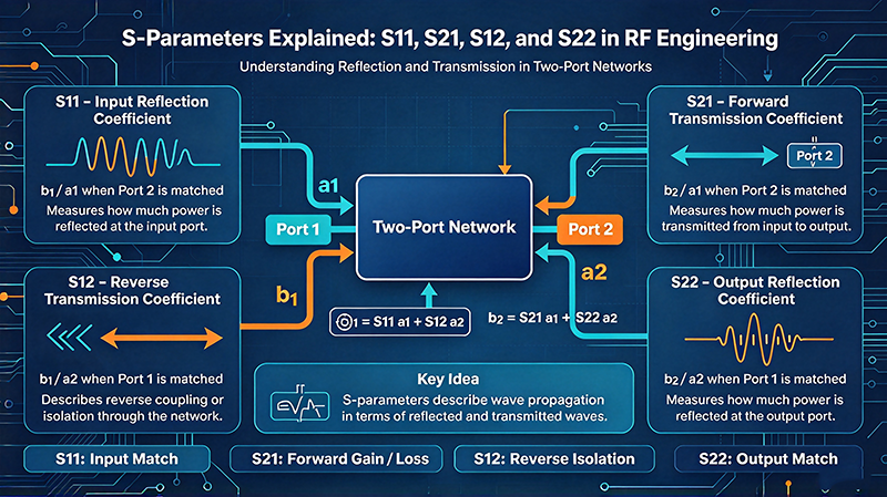
S-parameters — short for scattering parameters — are the universal language used to describe how radio-frequency and microwave energy flows through a multi-port network. Rather than trying to measure voltages and currents at the ports of a device that may operate at tens of gigahertz (where voltmeters and ammeters become physically meaningless), S-parameters describe the device using the waves that travel into and out of each port. Each S-parameter is a complex number — both a magnitude and a phase — that expresses the ratio between an outgoing wave and an incoming wave at a specific frequency.
For a two-port device, which is by far the most common case in RF and microwave engineering, four S-parameters completely describe the linear behavior of the device across its operating frequency band. These are S11, S21, S12, and S22. Higher-order networks (three-port, four-port, etc.) have correspondingly more entries in their scattering matrix, but the principle is identical. Together, the four two-port S-parameters form a 2×2 matrix:
[S] = [ S11 S12 ] [ S21 S22 ]
Engineers measure S-parameters with a vector network analyzer (VNA), which stimulates the device with a known swept-frequency signal and uses directional couplers to separate incident and reflected waves. The resulting data can be presented as magnitude (in dB) versus frequency, as complex values on a Smith chart, or as time-domain reflectometry (TDR) responses.
S11 — Input Reflection Coefficient
S11 is the ratio of the wave reflected back from Port 1 to the wave sent into Port 1. It tells you how well the input port of your device is matched to the system impedance, almost always 50 Ω in test and instrumentation (75 Ω in cable TV and video). A perfectly matched device has S11 = 0 (no reflection), and a totally mismatched device (open or short) has |S11| = 1 (100% reflection).
In decibel form, S11 is closely related to return loss: RL(dB) = -20·log10(|S11|). A return loss of 20 dB corresponds to |S11| = 0.1, meaning only 1% of the incident signal is reflected. For most RF and microwave designs, a return loss of 15 dB or better is considered acceptable, while 20 dB or better is good.
When designing an antenna, a filter, or an amplifier input stage, S11 is the first specification you look at. It directly determines standing-wave ratio, radiated efficiency, and — for receivers — the noise figure contribution of the input match.
S21 — Forward Transmission / Gain / Insertion Loss
S21 is the ratio of the wave coming out of Port 2 to the wave sent into Port 1. It is the classic metric for insertion loss in passive devices (filters, attenuators, cables) and for gain in active devices (amplifiers). A low-loss filter has S21 close to 0 dB in its passband; a typical LNA might have S21 between 15 and 25 dB; a cable with 3 dB of loss has S21 = -3 dB.
Because S21 describes how much signal actually makes it from input to output, it directly sets the link budget for any system. A filter that loses 0.5 dB, a cable that loses 1 dB, and an LNA that adds 20 dB combine into a path that has -1.5 + 20 = +18.5 dB net gain. The math is additive in dB, which is one of the great conveniences of working in logarithmic units.
For active devices, S21 is also called small-signal gain. It is measured with the input power backed off enough that the device remains in its linear region — typically 10 to 20 dB below the 1 dB compression point. Pushing the device into compression changes its effective S21 and breaks the linearity assumption that makes S-parameters useful in the first place.
S12 — Reverse Transmission / Isolation
S12 is the ratio of the wave coming out of Port 1 to the wave sent into Port 2. It is the reverse-direction counterpart of S21, and for most passive devices it is very similar in magnitude to S21 (a symmetric filter has S12 = S21). For amplifiers and active switches, however, S12 is often much smaller than S21 and is referred to as reverse isolation.
Reverse isolation matters because it determines how much output-side impedance variation or load mismatch couples back to the input. A high-isolation LNA (S12 < -40 dB) is immune to load changes at its output; a low-isolation amplifier (S12 = -20 dB) can oscillate if its output is even slightly mismatched. In switches, S12 (or S32, S42, etc. for multi-throw switches) describes how well an OFF port is isolated from the COMMON port. Better switches have S12 of -80 dB or lower at the operating frequency.
S22 — Output Reflection Coefficient
S22 is the ratio of the wave reflected back from Port 2 to the wave sent into Port 2. It indicates how well the output port of your device is matched to the load impedance. The same thresholds apply as for S11: an S22 of -15 dB or better is generally acceptable, and -20 dB is good.
For an amplifier, S22 is set by the output matching network and the device's intrinsic output impedance. For an antenna, S22 is the same as S11 because the antenna is a one-port device. For a filter, S22 typically matches S11 in the passband but differs sharply in the stop-band (where one port may be matched while the other is reflective).
How to Read an S-Parameter Plot
S-parameter data is presented in several formats, each suited to a different analysis. The most common is the log-magnitude plot: S21 in dB on the y-axis versus frequency on the x-axis. A flat curve near 0 dB across the operating band means excellent transmission; a deep notch (e.g., -60 dB at a specific frequency) indicates a filter stop-band. The slope and ripple of the S21 curve reveal pass-band flatness and group delay variation.
A Smith chart plots the complex reflection coefficient Γ on a circular grid, with constant-resistance circles and constant-reactance arcs. S11 and S22 are plotted as single points on the Smith chart at each frequency; a marker that hugs the center (Γ = 0) indicates a perfect match, while a marker that swings around the perimeter indicates a strong reflection. Smith charts are the natural tool for designing matching networks because adding a series reactance moves the marker along a constant-resistance circle, and adding a shunt susceptance moves it along a constant-conductance circle.
Time-domain reflectometry (TDR) presents the S11 data as if it were a one-shot pulse response: a discontinuity along a transmission line shows up as a reflection spike at the equivalent electrical distance. TDR is invaluable for diagnosing connector transitions, cable kinks, and PCB trace impedance discontinuities.
Multi-Port Networks and S-Matrix Symmetry
Devices with more than two ports — power dividers, couplers, circulators, MIMO antennas — have larger S-matrices. A 3-port device has 9 S-parameters (S11, S12, S13, S21, S22, S23, S31, S32, S33), a 4-port device has 16, and so on. Reciprocal devices satisfy Sij = Sji (the matrix is symmetric), and lossless devices require S†S = I (the matrix is unitary).
These mathematical properties are powerful design constraints. A directional coupler, for example, is a 4-port device whose S-matrix must have specific zero entries to provide the desired coupling and isolation. Trying to design such a device without the matrix-level view is essentially impossible.
Practical Tips for Working with S-Parameters
Always specify the reference impedance (typically 50 Ω), the measurement bandwidth, the number of points, the IF bandwidth (which sets the noise floor and speed tradeoff), and the calibration method (SOLT, TRL, or waveguide TRL) when sharing or comparing S-parameter data. Two S-parameter files that look identical in the plot can be measured under completely different conditions and may not agree in your application.
When importing S-parameters into a circuit simulator, use the Touchstone (.s2p, .s4p, .s8p) format, which preserves the complex data, the reference impedance, and the frequency grid. .csv files of magnitude-only data lose the phase information and are usually insufficient for cascade analysis.
Frequently Asked Questions
Q: What is the difference between S11 and return loss? A: They describe the same mismatch. S11 is a linear ratio (0 to 1), return loss is the same ratio with a minus sign converted to dB. S11 of 0.1 equals return loss of 20 dB.
Q: Can S21 be greater than 0 dB? A: Yes, in active devices such as amplifiers where the device adds power. For passive devices, S21 ≤ 0 dB because they cannot create energy.
Q: How are S-parameters related to Z-parameters and Y-parameters? A: They are mathematically equivalent representations of the same linear network, just expressed in different bases (waves, voltages/currents, or admittances). Most modern tools use S-parameters because they are easier to measure at high frequency.
Engineering Notes from the Lab
In practice, S-parameter measurement quality depends on three things the datasheet does not tell you: the quality of the calibration kit, the stability of the test cables, and the care taken with connector mating. A cheap calibration kit, or one that has been used so many times its standards have worn, will give you perfect-looking measurements that are actually wrong. Spend the budget on a high-grade kit (Keysight, Maury, or Rosenberger) and replace it when the verification standard drifts.
Connector mating is the most common source of measurement error. A properly torqued SMA connector at 8 in-lbs has the same impedance match as the cable it joins. A connector torqued hand-tight can have a 1.5:1 VSWR at 18 GHz — enough to introduce 0.5 dB of error in your S21 measurement. Use a torque wrench. Always.
Case Study: Filter Design Verification
A band-pass filter was simulated in software and predicted to have S21 of -1 dB at 2.4 GHz with -40 dB at 2.7 GHz. Measured on the VNA, the actual response was S21 of -1.4 dB at 2.4 GHz with -32 dB at 2.7 GHz. The discrepancy traced to (1) the SMA connectors' pin depth being slightly out of spec, (2) the test fixture adding 0.2 dB of insertion loss, and (3) the enclosure resonating at 2.65 GHz, which pulled the stop-band up by 8 dB. The fix: connector pin depth reset, de-embedding the fixture, and adding absorber material inside the enclosure.
Closing Thoughts
S-parameters are not just a measurement format — they are the contract between RF designers. When you publish or share a Touchstone file, you are telling your colleague or your customer exactly how your device behaves across frequency. Take the time to measure correctly, document conditions, and use the right format. The discipline you build into this process compounds across every project that follows.
Industry Applications and Use Cases
Across telecommunications, aerospace, defense, medical imaging, and automotive radar, the concepts covered in this guide show up in every RF design. From 5G base stations deploying massive MIMO antenna arrays with dozens of Wilkinson dividers per panel, to satellite payloads where every decibel of link budget determines the success of a multi-million-dollar mission, the principles remain the same: measure carefully, design with margin, and verify with the right instrument.
Medical applications add another wrinkle: MRI machines operate at the Larmor frequency of hydrogen (42.58 MHz/Tesla) and require extraordinarily low noise and high stability. Test systems for MRI receivers must minimize cable loss between the imaging coil and the low-noise preamplifier — often mounted directly on the coil housing — because every dB of loss degrades diagnostic image quality. The same matching, cabling, and LNA placement principles apply.
Automotive radar at 77 GHz is one of the fastest-growing RF domains. Each modern car may contain 5–10 mmWave radar units for adaptive cruise control, blind-spot detection, and automated emergency braking. These radar modules contain calibrated Wilkinson dividers, matched patch antennas, beam-steering phase shifters, and integrated FMCW synthesizers — all built on low-cost PCB substrates and tested in production at volumes exceeding 100 million per year. The principles taught in this guide are what make that volume manufacturing possible.
Advanced Design Considerations
Beyond the basics covered above, several advanced topics deserve attention as your designs mature. Multi-physics simulation — coupling electromagnetic, mechanical, and thermal effects in a single simulation — is increasingly important at mmWave frequencies where small dimensional changes from thermal expansion can shift the operating frequency. Tools like ANSYS HFSS, CST Studio Suite, and Cadence Clarity now include multi-physics capabilities that integrate structural and thermal solvers with the RF simulator.
Machine learning is beginning to appear in RF design. Surrogate models trained on simulation data can predict S-parameters 1000× faster than running the full EM simulation, enabling design space exploration that was previously impossible. Tools like Google Brain's RF antenna design work and Cadence's Cerebrus are early examples of where the field is heading. For now, these tools augment rather than replace the engineer's judgment — they accelerate iteration but the final design still needs to be understood, verified, and signed off by an experienced engineer.
Standards, Compliance, and Regulation
Every RF system must comply with applicable regulatory standards. In the United States, Part 15 of the FCC rules governs intentional radiators and unintentional emissions. The European Union's Radio Equipment Directive (RED) does similar work. Specific applications have additional standards: ETSI EN 301 893 for 5 GHz Wi-Fi, ETSI EN 302 500 for UWB, and many others. Military and aerospace applications have additional standards: MIL-STD-461 for EMI, MIL-STD-810 for environmental, and MIL-STD-1540 for product assurance.
Compliance testing is a discipline of its own. Compliance test labs use specialized instruments (spectrum analyzers with quasi-peak detectors, EMI receivers calibrated to CISPR standards) and follow specific procedures. The measurement uncertainty of compliance tests is typically ±3 to ±6 dB — much wider than production test measurements, but required for regulatory acceptance. Plan for compliance testing early in your design cycle; retrofitting a product to meet EMI requirements after the design is finalized is expensive and time-consuming.
Career and Skill Development in RF Engineering
RF engineering is a deep specialty with strong demand and excellent compensation. The barrier to entry is high: unlike software, you cannot iterate in seconds, and the cost of mistakes is paid in physical hardware. Yet for engineers who take the time to develop intuition, RF offers some of the most satisfying engineering work available — every component choice has a measurable effect, and every measurement reveals something about the physical world.
For those starting out, build a home lab. Even a modest setup with a cheap SDR (RTL-SDR, HackRF, or Airspy), a few antennas, and some cables will let you explore the RF spectrum in ways that no simulator can. Add a low-end spectrum analyzer (Rigexpert, TinySA) when you can afford it, and a used VNA from eBay when the budget allows. The hands-on experience with real signals, real cables, and real instruments is what builds intuition that no textbook can provide.
Stay current by reading industry publications (Microwave Journal, RF Globalnet, Microwaves & RF), attending conferences (IMS, EuMW, IEEE MTT-S), and joining professional communities (IEEE MTT-S, ACM SIGCOMM for networking RF). The field evolves rapidly — mmWave 5G, satellite internet, and automotive radar were niche markets 10 years ago and are now mainstream. The engineers who built those markets started by mastering exactly the fundamentals covered in this article.
About the Author — MeiXun Team
Chief Engineer Wang
High-tech Enterprise, Feifeng Talent
Chief Engineer Wang graduated with a master's degree in high-power microwave from the Institute of Electronics, University of Chinese Academy of Sciences.
View Full Profile- RF Switch Circuit Diagram
- RF Switch
- Ohm's Law
- dBm to Watt
- mW to dBm
- Wavelength to Frequency
- RF Connector
- SMA Connector
- RF Switch Module
- RF Coupler
- RF PIN Switch
- Microwave Coaxial Switch
- PIN Switch
- Coaxial RF Switch
- Waveguide Switch
- Microwave Switch
- Low Noise Amplifier
- PIN Diode Switch
- Coaxial Switch
- RF Microwave Switch
- SPST Switch