


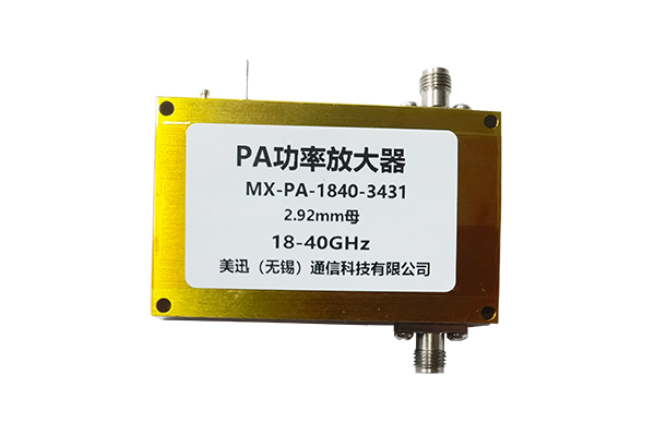
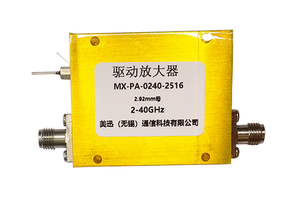




1. Why a limiter is non-negotiable in a high-power transmission path
In radar, electronic warfare (EW), satellite ground terminals, test equipment and industrial RF heating systems, the transmit chain routinely pushes tens to thousands of watts into the air or into a load. The receiver sitting next to it — often sharing an antenna through a duplexer or circulator — cannot see that power. A modern GaN LNA or SiGe mixer typically survives no more than +10 to +15 dBm of CW at its input; an accidental antenna short, a duplexer leakage spike, or a transmit pulse reflected through a faulty connector can deliver 50 V or more in less than a nanosecond.
A microwave limiter clamps that excess power to a safe ceiling before it reaches the fragile stage. Unlike an ordinary attenuator, which is a linear, lossy component, a limiter changes its own impedance with incident power: it looks like a near-short at high power and like a transparent, low-loss element at small signal. That dual behaviour is what makes it — and what makes it hard to design correctly.
2. How a microwave limiter actually works
Most limiters are built around one of two non-linear devices: a PIN diode (a silicon p-i-n junction whose intrinsic region becomes conductive under RF self-bias) or a Shottky-barrier / FET-based MMIC detector-and-shunt cell.
With a PIN limiter, the rectified RF current flows across the intrinsic layer, charges it, and pulls the diode from a high-impedance state into a low-impedance state within nanoseconds. The resulting shunt path reflects most of the incident power back toward the source and dissipates the rest as heat. Once the stimulus drops, stored charge must be cleared before the diode returns to high impedance — this defines the recovery time.
An active MMIC limiter integrates a detector, a low-frequency amplifier and a shunt FET on one die. It offers lower leakage and better temperature stability, but it needs bias, draws idle current, and usually cannot survive as much peak power as a well-matched PIN stage without additional external devices.
3. The parameters that actually define reliability
Vendors quote a long datasheet. In a high-power design, only a handful of numbers determine whether the limiter survives the next pulse.
| Parameter | What it really means | Design implication |
|---|---|---|
| Flat leakage level | Output power when the limiter is fully driven into clamp (CW or long pulse). | Sets the safe operating point for the LNA/mixer behind it. |
| Peak / threshold power | Incident power at which clamping begins (typically +10 to +17 dBm). | Must be above receiver compression so desired small signals pass unattenuated. |
| Power handling (CW / pulsed) | Maximum incident power the device can absorb without destruction, in W or dBm. | Derate by 50% against your worst-case reflected + coupled energy. |
| Insertion loss | Small-signal attenuation through the device (0.3–1.5 dB typical). | Directly subtracts from receiver noise figure. |
| Response / recovery time | Time to clamp, and time to release after the pulse ends (ns to µs). | Determines how much energy leaks during fast transients and how quickly the receiver returns to sensitivity. |
| VSWR / return loss | Input and output match in the small-signal state. | Poor match degrades duplexer isolation and LNA stability. |
4. Choosing the right limiter topology
There is no single "best" limiter. The right topology depends on how much power you must absorb, how fast it arrives, and what leakage you can tolerate.
- Passive PIN-diode limiter. Highest peak power (100 W to kW range), no bias rail, fastest response on the order of nanoseconds. Trade-offs: higher flat leakage, temperature-sensitive threshold, longer recovery after long pulses.
- Active MMIC limiter. Low leakage (often < +10 dBm), flat over temperature, fast recovery. Trade-offs: finite peak power (~+20 to +30 dBm), requires bias and bypass decoupling, more sensitive to ESD.
- Hybrid (cascaded) limiter. A passive PIN stage at the antenna absorbs the bulk energy; a low-leakage MMIC stage behind it cleans up the residual clamp. This is the standard architecture for wideband radar and EW front-ends above 6 GHz.
- GaN-based limiters. Emerging class that pushes peak power to the 100–500 W region with sub-nanosecond response; useful where size and weight prohibit a bulky circulator + external limiter combination.
5. The 8-step design flow
Treat the limiter as a system block, not as a part number you pick from a catalog. The following sequence is the one we apply to every new front-end.
Capture the threat model
List every possible incident at the limiter input: CW carrier, pulsed radar envelope, VSWR mismatch, nearby transmitter coupling, ESD/EMP, and lightning surge. Note peak power, average power, pulse width, duty cycle and repetition rate.
Define the protection window
From the downstream device's absolute maximum rating, set flat leakage and peak clamp targets with 6 dB / 3 dB margins. Specify recovery time so the receiver is ready before the next pulse arrives.
Pick topology & device family
Match power handling to the largest threat, leakage to the LNA rating. Choose between PIN, MMIC, hybrid or GaN. Prefer parts that already cover your full frequency band rather than cascading two narrowband devices.
Budget noise figure and linearity
Insertion loss of the limiter plus any preceding switch sets the system noise figure. Verify the small-signal 1-dB compression point still leaves headroom for your own wanted signal through the limiter path.
Thermal and derating plan
Compute junction temperature from absorbed power and θJC + θCA. Apply at least a 50% derating on peak power and 80% derating on average power for continuous operation.
Lay out for RF, not for convenience
50 Ω controlled-impedance lines, shortest possible shunt paths, multiple vias under each ground pad, and a continuous ground plane. See section 7 for the checklist.
Simulate, then prototype twice
EM-simulate the package and surrounding copper. Build an engineering sample, then a second revision based on measured leakage and recovery — first-pass silicon is almost never the production part.
Qualify against the threat list
Pulse the limiter to its rated peak power, step the VSWR to 10:1, run temperature cycles, and re-measure small-signal S-parameters. Any drift in insertion loss or threshold is a red flag.
6. Thermal design and derating
Failure in a microwave limiter is almost always a thermal failure, not an electrical one. When the limiter clamps, the incident power it does not reflect is converted to heat in the intrinsic region of the diode or in the FET channel. For a PIN device, that heat has to escape through the package, the pad, the copper pour and the board.
Use the following check list before approving a layout:
- Pad the limiter with a copper pour at least 3× the device footprint on each side, and add plated thermal vias (0.3 mm drills on 0.6 mm pitch) from the top pad to the internal ground plane.
- Do not rely on a single-layer 1 oz copper pour for >5 W average dissipation; stack two or more ground layers.
- For pulsed threats, model the junction temperature as a thermal RC rather than an average — a 1 kW, 1 µs pulse still dumps 1 mJ, and repeated at 10 kHz it produces 10 W of average heating.
- Keep the limiter away from LDOs, power inductors and the PA's heat sink. A 20 °C ambient rise at the package shifts the limiter threshold by several dB and accelerates aging.
7. PCB layout rules that make or break reliability
A perfect limiter on a bad board is just an expensive resistor. High-power RF layout is mostly about controlling the shunt path to ground.
- Keep shunt devices directly across the line. The pad of a shunt diode should connect to the ground plane with the shortest, widest via possible. Even 0.5 mm of stub inductance shifts the clamp frequency and spikes leakage.
- Maintain 50 Ω from antenna to limiter to LNA. Use a controlled impedance stack-up, do not change layer halfway through the protection network, and keep reference planes continuous under every signal trace.
- Decouple active limiters locally. Place a 100 pF RF capacitor and a 10 nF bulk capacitor within 1 mm of the bias pin, with their own vias to ground. A long bias trace becomes an RF pick-up and an unwanted shunt path.
- Separate high-power and low-sensitivity sections. Keep the transmit side of the duplexer at least 5 mm away from the limiter + LNA board area, and put a grounded guard trace between them.
- Use ESD cells, not fuses. A fuse reacts in milliseconds; an ESD event ends in nanoseconds. Add a dedicated TVS or Schottky ESD diode at the connector-facing edge of the board.
- Mark and label the protection chain. Silkscreen the limiter, the ESD cell and the LNA input on the assembly drawing. Field engineers diagnosing a dead receiver should be able to probe each stage without removing shields.
8. Validation and test — what to actually measure
A datasheet curve is a starting point, not a guarantee. On every production design, bring up the limiter on a bench that can reproduce the threat list.
- Small-signal S-parameters (S11, S21, S22) across the full band, hot and cold, to confirm insertion loss and match.
- Transfer curve: sweep input power from −10 dBm to the rated peak and plot output power. The knee must be well defined and flat leakage must sit below your budget.
- Pulsed response: feed the rated pulse at the worst-case duty cycle and capture output leakage with a fast oscilloscope. This is where recovery time and tail-of-pulse leakage show up.
- VSWR robustness: insert a tuner at the output and step the reflection coefficient up to 1.0 at every phase angle. A limiter that works into a matched load but fails at 10:1 VSWR is not ready.
- Endurance: run 106 pulses at the rated power and re-measure S-parameters. Any drift in threshold or insertion loss points to latent damage.
9. Common design pitfalls
- Sizing from CW power only. Pulsed systems must be sized from peak pulse voltage, not average power. A 100 W peak at 1% duty cycle is still 100 W peak.
- Forgetting the recovery tail. If the limiter has not recovered before the next receive window, your receiver sensitivity collapses just when you need it most.
- Single-point-of-failure protection. One limiter stage carrying the entire threat is a reliability gamble. Two cascaded stages share the energy and survive the failure of one.
- Ignoring the bias network. An active limiter with a poorly decoupled rail becomes a parasitically oscillating oscillator, not a protector.
- Trusting first-pass silicon. Package parasitics and board coupling always differ from the simulation. Plan two prototype turns.
10. Frequently asked questions
What is the difference between a limiter and an attenuator?
An attenuator is a linear, fixed-loss component. A limiter is non-linear: it presents low insertion loss at small signal and automatically drops to a low-impedance, high-loss state when incident power exceeds its threshold. It protects downstream circuitry instead of merely reducing every signal equally.
Can a microwave limiter replace a circulator?
No. A circulator provides continuous, broadband isolation between transmitter and receiver based on magnetic biasing; a limiter only clamps transient excess power. In high-power systems they are used together — the circulator handles steady-state isolation, the limiter catches the spikes and reflected energy the circulator cannot fully suppress.
How much insertion loss is acceptable for a limiter?
For most receive chains, 0.3 to 1.0 dB is acceptable. Loss above 1.5 dB directly degrades noise figure and usually signals that you have over-specified the protection stage. If you need less loss than a given limiter provides, move the protection closer to the antenna so the LNA itself sits after the limiter in the low-loss position.
How do I choose between a PIN diode and an MMIC limiter?
If the dominant threat is high peak power (tens to hundreds of watts), start with a passive PIN limiter. If the dominant requirement is low leakage and fast recovery at modest power, choose an active MMIC. For demanding radar and EW platforms, combine the two in a cascade: PIN for energy absorption, MMIC for leakage cleanup.
What derating factor should I apply?
As a starting point, derate peak power handling by 50% against your worst-case incident energy and derate average power by 20%. Then re-check the junction temperature at the maximum case temperature and tighten the derating if the silicon gets close to its rated TJ.
Is an ESD diode enough to protect the LNA?
An ESD diode handles short electrostatic discharges but cannot absorb transmitter-level energy. It belongs after the limiter, as a final safety net for handling and connector-level surges, not as the primary protection.
11. Summary
Designing a reliable microwave limiter is a system exercise, not a component selection. Start from the threat model, size the leakage and peak clamp with margin, choose a topology that matches both, derate aggressively on power and temperature, and validate the design under the worst-case VSWR and pulse conditions the product will ever see. Done this way, the limiter becomes the invisible, trusted block that lets the rest of the high-power transmission system run for years without a field return.