


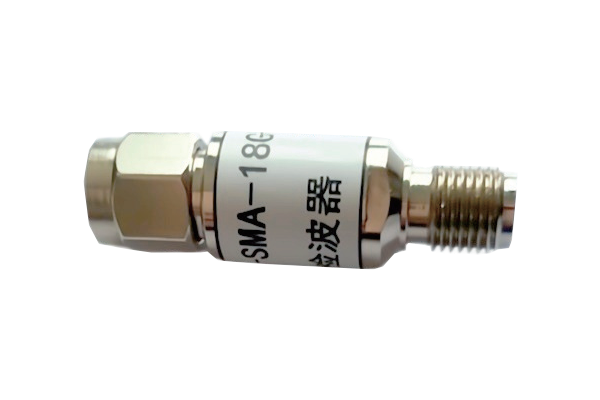
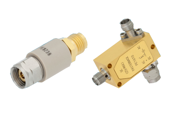


What is the working principle of PIN diode switch
The PIN diode switch is an electronic switch based on the characteristics of PIN diode. Its working principle is as follows:
The PIN diode is composed of a layer of intrinsic semiconductor (I layer) inserted between the P-type semiconductor and the N-type semiconductor. When forward biased, that is, the P terminal is connected to a positive voltage and the N terminal is connected to a negative voltage, the external electric field causes the holes in the P region and the electrons in the N region to be injected into the middle I layer. Due to the existence of the I layer, the injected carriers accumulate in the I layer, which greatly increases the conductivity of the I layer and presents a low resistance state. At this time, the PIN diode is equivalent to being turned on, allowing current to pass, just like a closed switch.
When reverse biased, the P terminal is connected to a negative voltage and the N terminal is connected to a positive voltage. The external electric field causes the holes in the P region and the electrons in the N region to move further away from the I layer. There are almost no carriers in the I layer, which is in a high resistance state, with only a small reverse leakage current, which is equivalent to the switch being disconnected, preventing current from passing.
In the PIN diode switch circuit, the switching function is realized by utilizing the characteristic of the PIN diode that it presents different resistance states under forward and reverse bias. By controlling the polarity and size of the bias voltage applied to the PIN diode, its conduction or cutoff can be controlled, thereby realizing the on-off control of the signal path. For example, in RF circuits, PIN diode switches are often used to switch different RF signal paths, control the transmission and blocking of signals, etc. They have the advantages of fast switching speed, low insertion loss, and high isolation, and can meet the requirements of various high-speed and high-frequency signal processing circuits.