How to use pin diode switch to control bias
PIN Diode Switch Biasing Control
Biasing control of a PIN diode switch involves adjusting current/voltage to switch between "on" and "off" states while maintaining signal integrity.
Forward Biasing (On State)
Bias: Positive voltage (anode > cathode)
Current Range: Several mA to hundreds of mA
Result: Low resistance (~closed switch)
- Carriers injected into intrinsic (I) layer reduce resistance
- Bias network must provide low RF impedance
- Current must avoid overheating while ensuring full conduction
Reverse Biasing (Off State)
Bias: Negative voltage (5-30V typical)
Requirement: Below breakdown voltage
Result: High resistance (~open circuit)
- I-layer depletes carriers, increasing resistance
- Bias network needs high RF impedance
- Resistors/bias tees separate DC and RF paths
Bias Network Design
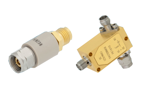
- Bias tees: Combine DC and RF paths while preventing interference
- RF chokes: Block RF signals while passing DC bias
- Decoupling capacitors: Suppress high-frequency noise on DC lines


