


How to resist interference with low-noise amplifier
LNA Anti-Interference Design Techniques
A low-noise amplifier (LNA) employs several strategic design techniques to mitigate interference and ensure reliable signal amplification in noisy environments.
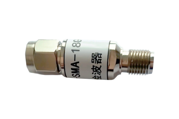
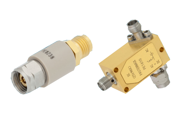
LNAs integrate input matching networks or pre-filters to restrict bandwidth, allowing only the desired frequency band to pass while blocking out-of-band interference.
In RF applications, a band-pass filter at the input suppresses unwanted signals (adjacent channel noise, EMI) while ensuring only the target frequency is amplified, reducing intermodulation distortion.
Precise impedance matching between the LNA's input stage and source minimizes signal reflections and maximizes power transfer.
- Uses stub matching or π-network filters
- Aligns input impedance with source impedance
- Reduces interference coupling
- Improves signal purity
Choosing transistors with inherently low noise characteristics is critical for interference rejection.
- Silicon germanium HBTs or GaAs PHEMTs for RF
- Operate with minimal thermal and shot noise
- Careful biasing at "minimum noise" point
- Optimizes noise performance
Physical design considerations to minimize noise coupling.
- Compact, shielded layouts
- Ground planes and metal shielding
- Minimizes parasitic capacitances/inductances
- Differential amplifiers reject common-mode noise
Handling strong interfering signals without saturation.
- Automatic Gain Control (AGC)
- Limiting stages maintain linear range
- Prevents overload from large unwanted signals
- Preserves weak desired signals
Through these comprehensive techniques, LNAs achieve robust anti-interference capabilities, ensuring reliable signal amplification even in challenging electromagnetic environments while maintaining excellent noise performance.