


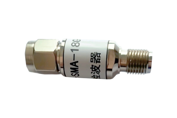


How to reduce the insertion loss of an RF pin diode switch
Optimizing RF Pin Diode Switches
Key strategies to minimize insertion loss and enhance performance in RF switching applications
Select High-Quality RF Pin Diodes
- Prioritize diodes with low on-resistance to minimize signal attenuation
- Choose diodes made of gallium arsenide or silicon carbide for better conductivity
- Select diodes with tight manufacturing tolerances for consistent performance
- Avoid standard silicon diodes when lower parasitic reactances are critical
Optimize Circuit Design
- Minimize signal path length to reduce resistance and radiation loss
- Use high-conductivity PCB materials with thick copper layers
- Avoid sharp bends in signal traces to prevent impedance discontinuities
- Integrate bypass capacitors close to diode bias pins
Ensure Precise Impedance Matching
- Design circuits to match characteristic impedance (typically 50Ω in RF systems)
- Use impedance-matching networks with inductors, capacitors, or transmission line stubs
- Conduct thorough impedance testing during circuit development
- Adjust matching components to eliminate reflections and ensure maximum signal transfer
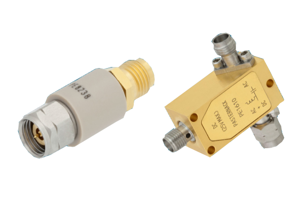
Improve Heat Dissipation & Package Design
- Integrate heat sinks or thermal vias to maintain stable operating temperature
- Choose packages with low parasitic inductance and capacitance
- Ensure secure electrical connections with minimal contact resistance
- Regularly inspect and maintain switches to prevent dust accumulation and corrosion