How to optimize the insertion loss of PIN diode switch
Device selection
Select PIN diodes with low parasitic parameters. The parasitic capacitance and series resistance of the PIN diode itself are important factors leading to insertion loss. Low parasitic capacitance can reduce the bypass loss of high-frequency signals, and low series resistance can reduce the ohmic loss of the signal in the on state. Select devices with appropriate rated current and reverse breakdown voltage so that they can operate stably under actual working conditions and reduce unnecessary losses.
Circuit design
Optimize bias circuit. Reasonably design the bias circuit to ensure that the PIN diode obtains a stable and appropriate bias current so that the diode works in the best on state. Avoid bias current that is too large or too small, otherwise it will increase insertion loss.
Perform impedance matching. At the input and output ends of the switch circuit, by reasonably designing the matching network, such as using a matching circuit composed of microstrip lines, inductors and capacitors, the impedance of the switch is matched with that of the previous and next stage circuits, reducing reflection loss and improving signal transmission efficiency.
Reduce wiring length. In PCB design, try to shorten the wiring length between the PIN diode switch and other circuit components, reduce the influence of wiring resistance and parasitic inductance and capacitance, and thus reduce insertion loss.
Heat dissipation management
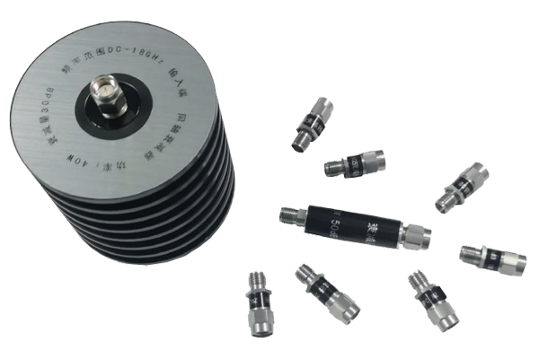
The PIN diode will generate a certain amount of heat during operation. Excessive temperature will cause its performance to degrade and insertion loss to increase. Therefore, effective heat dissipation measures should be taken, such as adding heat sinks and optimizing the heat dissipation layout of the PCB, to ensure that the diode works within a suitable temperature range and maintain its low loss characteristics.
Process manufacturing
During the manufacturing process, ensure the packaging quality and process accuracy of the PIN diode. Good packaging can reduce the influence of parasitic parameters and improve the performance of the switch. At the same time, precise manufacturing processes help to ensure the consistency and stability of the diode and reduce the fluctuation of insertion loss.


