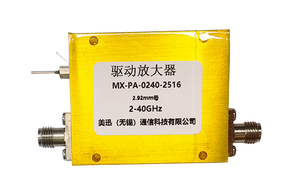
How to Improve Interference Resistance in RF Low-Noise Amplifiers
Optimizing Circuit Layout and Component Selection
During the circuit design phase, the component layout and signal path of the RF Low Noise Amplifier must be carefully planned.
Sensitive low-noise amplifier modules should be placed separately from high-interference source components to avoid close proximity and interference coupling.
At the same time, prioritize components with excellent anti-interference performance, such as transistors with low noise figures and good shielding, and passive components with low parasitic parameters, to reduce the possibility of interference introduced by the components themselves.
Furthermore, shortening key signal transmission paths reduces the probability of external interference during signal transmission, thereby improving the anti-interference foundation from the very beginning of the design.
Strengthening Electromagnetic Shielding
Block the intrusion of external interference signals through electromagnetic shielding. Enclose the entire RF Low Noise Amplifier or core module in a metal shielding case.
The shielding case must have good conductivity and sealing properties to ensure effective reflection or absorption of external electromagnetic radiation.
Seams within the shielding case must be properly sealed to prevent gaps that reduce shielding effectiveness.
Furthermore, shielded cables can be used for signal lines susceptible to interference, and the shielding layer must be reliably grounded to further minimize the impact of external electromagnetic interference on signal transmission.
Adding High-Efficiency Filtering Circuits
Add filtering circuits to the RF Low Noise Amplifier's power supply, signal input, and output terminals.
The power supply filtering circuit can utilize an appropriate combination of capacitors and inductors to filter out high-frequency interference and voltage fluctuations introduced by the power supply line, providing the amplifier with a stable and clean power supply.
The signal port's filter circuitry should be designed with a targeted bandpass or lowpass filter structure based on the amplifier's operating frequency band.
This allows the desired signal to pass smoothly while suppressing out-of-band interference signals from entering the amplifier, preventing them from overlapping with the desired signal and impacting amplification performance.
Optimize Grounding System Design
Build a reasonable grounding network to reduce interference introduced by ground loops in the RF Low Noise Amplifier system.
Use single-point or multi-point grounding to separate the amplifier's signal, power, and shield grounds to prevent interference from different types of ground currents.
Ensure that the ground traces are short and thick to reduce ground resistance, minimize voltage drop across the ground trace, and prevent interference signal coupling caused by poor grounding.
Furthermore, reliably connect the amplifier ground terminal to the system ground grid to establish a unified ground reference point, further enhancing overall anti-interference capabilities.


