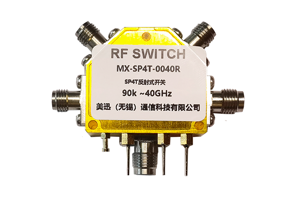
The PIN diode switch is a crucial component in many electronic systems, especially in RF and microwave applications. Its working principle is based on the unique characteristics of the PIN diode under different biasing conditions.
When a forward bias is applied to the PIN diode, that is, the P - region is connected to the positive terminal and the N - region to the negative terminal, a large number of carriers (electrons and holes) are injected into the intrinsic I - layer. This injection significantly increases the conductivity of the I - layer, causing the PIN diode to exhibit a low - resistance state. In this state, the PIN diode switch is equivalent to being closed, allowing RF signals to pass through with little attenuation.
Conversely, when a reverse bias is applied, with the P - region connected to the negative and the N - region to the positive, the carriers in the I - layer are extracted, forming a depletion layer. As the reverse voltage increases, the width of the depletion layer expands, and the PIN diode shows a high - resistance state. In this case, the capacitance of the diode becomes very small, and it presents a significant impedance to RF signals, effectively blocking their transmission. Thus, the PIN diode switch is equivalent to being open. In summary, by controlling the biasing voltage of the PIN diode, its resistance can be changed, enabling it to function as a switch for RF signals, facilitating the control and routing of signals in various electronic systems.


